GOWIN Semiconductor’s ARM-based FPGA SoC, GW1NS-2K, for smart connected devices, portable consumer and IoT, AI and edge computing
GOWIN Semiconductor has unveiled Gowin first FPGA SoC devices of the LittleBee family GW1NS series, GW1NS-2. The chip leverages the advantages of FPGA (field programmable digital array) programmable features to enable customers to design the interfaces and peripherals they need in different applications scenarios with the integrated 1.7K LUTs low power FPGA logics, and configure these peripherals with the embedded CPU. By directly integrating the data processing function of CPU with low-density FPGA into one FPGA SoC system, the chip opens a new frontier of FPGA applications and systemization, the company said.
GW1NS-2 is claimed as the first devices in the FPGA industry to integrate Cortex-M3 MCU and 1.7K LUTs logic in a single FPGA SoC.
The low-density, non-volatile, embedded flash memory FPGA devices is ideal for applications such as consumer, industrial control, IoT and security.
GW1NS-2K FPGA SoC
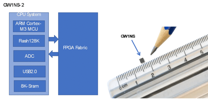
GW1NS-2 FPGA SoC device features an embedded ARM Cortex-M3 hardcore processor and integrated USB2.0 PHY, user flash, SRAM read/write controller and ADC converter, providing customers an all-in-one embedded solution with programmable logic features in one chip.
“GW1NS-2 FPGA SoC device fully utilizes the complementary features of MCU and FPGA, together with flexible peripherals of USB PHY and ADC, which widely extends the FPGA markets and applications. The availability of GW1NS-2 is also the prologue of Gowin strategy on AI and the emerging edge computing market. GW1NS series is the ideal embedded processor solution with programmability to address the applications like pattern and voice recognition in AI (artificial intelligence) and edge computing endpoints”, the company noted.
With Gowin integrated development environment, engineers can develop their hardware and software in a single platform, which is another innovation of FPGA design platform and reduces engineering design cycle.
According to the company, GW1NS-2 provides features like high-performance logic, low power consumption, high IO to logic ratio, instant-on, non-volatile, high security, abundant package option, high design flexibility and low-cost features.
GW1NS-2 FPGA SoC devices offer seamless connection between programmable logic devices and embedded processor, compatible with a wide range of peripheral devices standard and reduce system cost significantly.

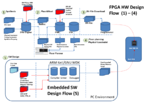
As shown in Figure1, the application development of GW1NS-2 FPGA SoC integrates hardware and software design flow, i.e., FPGA hardware logic design flow and embedded processor software design flow.
The primary objective of FPGA SoC design is to configure the FPGA logic elements to be various physical peripherals of the embedded processor (CPU). After completing the architecture and hardware design with the FPGA logic, engineers can do embedded processor software programming to configure these peripherals.
Gowin provides GW1NS-2 FPGA SoC devices and driver library, combining the software design tools (Compiler, Linker, Debugger) in an integrated development environment to support GW1N2-S FPGA SoC embedded processing programming; and also support ARM-MDK and GNU software design tools.
“Gowin Semiconductor always focus on product advantages accumulation, innovation and differentiation”, said by Stanley Tse, Reginal Sales Director of Gowin Semiconductor Corp, “The official launches of GW1NS-2 is our first trial on SoC market with our proven success LittleBee FPGA family + ARM hardware architecture. With this based architecture, we integrate high speed MIPI DPHY, ADC and other applications modules; together with our advantages on small package and low cost. We are very confident on market acceptance of GW1NS-2 and create another tremendous success of LittleBee family in broad range of applications, e.g., video interface, smart connected devices, portable consumer and ioT, AI and edge computing endpoints.”
Engineering samples and development boards for the GW1NS-2K are available.
For more information about GOWIN, click here.


