
Choose unframed or “cut” stencil while doing prototyping, it is cheaper and can be shipped easily as compared to framed stencils.
Curated by Vinay Prabhakar Minj

To ensure that an idea of a product is workable, it is very important for a developer to go through prototyping. However, prototyping involves several challenges such as:
- Limited resources
- Budgetary constraints
- Limited time to market
- Non-trivial level of complexity
Use of pre-built modules (e.g. IoT hardware) can make prototyping less complex if your aim is limited to proving the concept or idea. But if you want to go to the next stage, designing your own PCB with SMT components so as to move towards the actual product, you will need to grapple with the issue of SMT prototyping.
SMT mayhem
Surface-mount technology (SMT) is a method for producing electronic circuits in which the components are mounted or placed directly onto the surface of printed circuit boards (PCBs). (definition by Wikipedia)
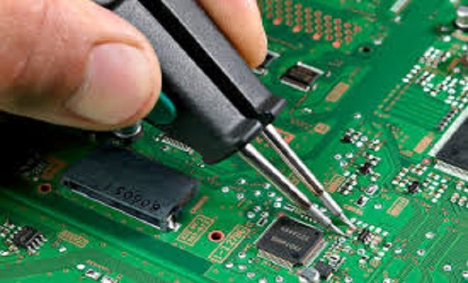
SMT mayhem refers to the errors that may occur while trying to solder an SMT component with the help of soldering iron. Due to SMT’s small size, precise soldering is required.
SMT assembly with tweezers and soldering tools is not easy as pie but far from it. The manual skills and steady hand are not easy to come by.
Prototyping strategies
There are two approaches to prototyping:
- Divide and conquer approach – It involves building and testing a sub-circuit. This method is more common use during early stages of prototyping. Partial assembly can speed up the overall prototyping process and gets you to market faster.
- Big bang approach – It involves building and testing a completely assembled PCB. This method is suitable for the late stage of prototyping.
Activities in prototyping
- Design circuit schematics – Start with this by choosing the required components.
- Design PCB layout
- Fabricate PCB
- Assemble PCB
- Test the PCB
Sometimes, one may have to go through several rounds of prototyping and rework on the above activities. i.e.
- Modifying schematic design
- Modifying the PCB layout
- Re-fabrication or re-assembling the PCB
- Replacing parts
- Assembling a new PCB
Some of the above processes could take a lot of time, and thereby increasing the product’s time to market. These are the bottlenecks in the process of prototyping. It is critical to have fast turn-around in prototyping. Cycle time can make it or break it. Therefore, the iterative process should be lessened as much as possible.
SMT PCB assembly process
It can be divided into three stages. The first stage is as follows:
- Lay the PCB right side up and put the stencil on top of it.
- Adjust until the alignment between them is good.
- Apply solder paste.
- Examine solder paste coverage.
- Remove the stencil without smudging.
The second stage is as follows:
- On the wet PCB pad, pick and place components. While doing so, make sure that:
- Parts are correct.
- Polarity/orientation is correct.
- Don’t let solder paste dry up, else the PCB will not come out as good.
- If doing manually with the help of tweezers, then don’t let the parts fly.
- Then put the PCB with properly placed components into the reflow oven. If not properly heated, then remove the PCB and inspect it for any component issues.
The third stage is as follows:
- To finish up, softly brush and clean the PCB with Iso-Propyl Alcohol (IPA).
- Test for any power shorts before doing a power-up test.
SMT assembly tips
- It is suggested to go for unframed or “cut” stencil while doing prototyping. It is cheaper as compared to framed stencils that are heavy in weight and expensive to ship.
- Ensure to make fewer mistakes as handling and placing of SMT components on a PCB is not easy.
- Usually, outsourcing for PCB fabrication is good in order to save money and time. PCB fabrication is a specialised job as it involves usage of hazardous chemicals. Therefore, safety is another reason for which outsourcing should be done.
- Make sure to inspect results carefully as a PCB passed-off as “100% tested” may not be so.
- For pasting and cooking, use good “lead-free” paste.
Typical errors/mistakes
- Incorrect design/layout issues.
- Not sufficiently testing the access points i.e. probe points.
- Not doing sufficient repair works.
- Components not used as per design.
- Incorrect placement of components.
- Incorrect orientation of polarities of components.
- Poorly rated part used.
Reducing cycle time with in-house assembly
Make sure to follow the below methods at an early stage of prototyping.
- If there is an assembly error, rework one or entire batch.
- If there is a PCB fabrication error, then re-fabricate the PCB.
- If there is a schematic error, then redo the layout procedure of the components.
Benefits of in-house SMT prototyping
- It gives increased/early visibility into all aspects of design issues e.g. mechanical issues, thermal issues.
- It prepares for DFM (Design For Manufacturing) and productization.
- It provides total control over intellectual property.
- It results in design and BOM (Bill Of Materials).
Benefits of partial assembly and incremental prototyping through hardware-software co-design
- Testing your hardware “piece-by-piece” with the help of software can reduce the cycle time.
- Doing sub-circuit level prototyping with the help of software can again reduce cycle time.
- Using software can help in skipping some expensive parts (when not needed in the first level of testing) such as connectors, peripherals.
- Speeds up initial bring-up of proto and test boards.
- Reduces unpredictability arising from external factors.
- Reduces overall product development cost and time.
Some general Design For Prototyping (DFP) tips
- Provisional of fuses (final product may or may not include these).
- Use zero ohms resistors or fuses to isolate power paths.
- Have all above DFP additions with 0805 footprints. This will make them “tweezer-friendly”.
- Add test points liberally. Small pads of 0.5 x 0.5mm will do for occasional probing.
- Where it is needed to permanently hook-up a test probe, add a thru-hole pin pad.
- Use rounded pads in footprints for small passive components and ICs.
- Be careful with big thermal pads.
- Prefer non-BGA (Ball Grid Array) packages if possible.
- Include fiducial marks in stencil for easy registration.
- Slightly undersize the stencil openings.
Equipment and process support
- Have auto pick and place.
- Have a good PCB reflow oven.
- The equipment should do 0402, cut tape and fine pitch ICs.
SMT prototyping can be challenging. So, build in-house assembling capability to cut cycle-time/cost, use DFP (Design For Prototyping) guidelines and deploy appropriate equipment and process.
About the author
This content is an extract from a speech presented by Ajith Narayanan, Co-founder of Zoid Labs, at IOTSHOW.IN 2019. Narayanan has several decades of experience in R&D and product development involving electronics, embedded systems and systems software.
Earlier he had worked with HCL R&D and C-DOT in India, as well as in Europe and Singapore, with multinational companies including Xerox, Digital Equipment and IBM.


